Wafer Bonding For Silicon On Insulator Technologies

Silicon On Insulator Soi Market Insulation Marketing Semiconductor

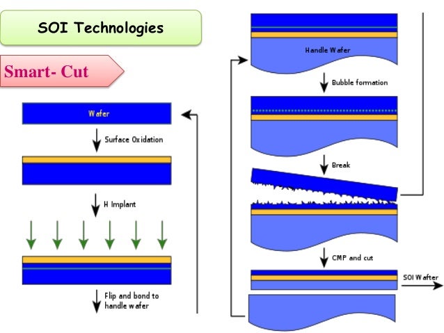
Schematic Of The Smart Cut Tm Technology Www Soitec Com Download Scientific Diagram

Pdf Silicon On Insulator Technology Review
Silicon On Insulator Soi Technology

Semiconductor Device And Processing Technology Ppt Video Online Download

Silicon On Insulator An Overview Sciencedirect Topics

Wafer bonded cmuts can be fabricated by fusion bonding a silicon and a silicon on insulator soi wafers fig.
Wafer bonding for silicon on insulator technologies.

What Are Soi Wafers Or Silicon On Insulator Wafers

Development Characterisation And Simulation Of Wafer Bonded Si On Sic Substrates Sciencedirect

Smart Cut Technology Smart Choice Soitec
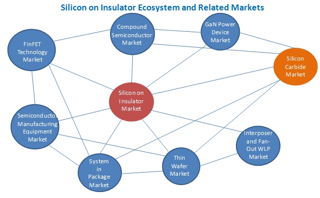
Silicon On Insulator Soi Market By Wafer Size Wafer Type Technology Product Covid 19 Impact Analysis Marketsandmarkets

Pdf Silicon On Insulator Technology For Microelectromechanical Applications

Main Steps Of The Layer Transfer Technique Used To Transfer The Download Scientific Diagram
Silicon On Insulator Waveguides Springerlink

Lees Process Integration Of Iii V Gan And Cmos A A Download Scientific Diagram
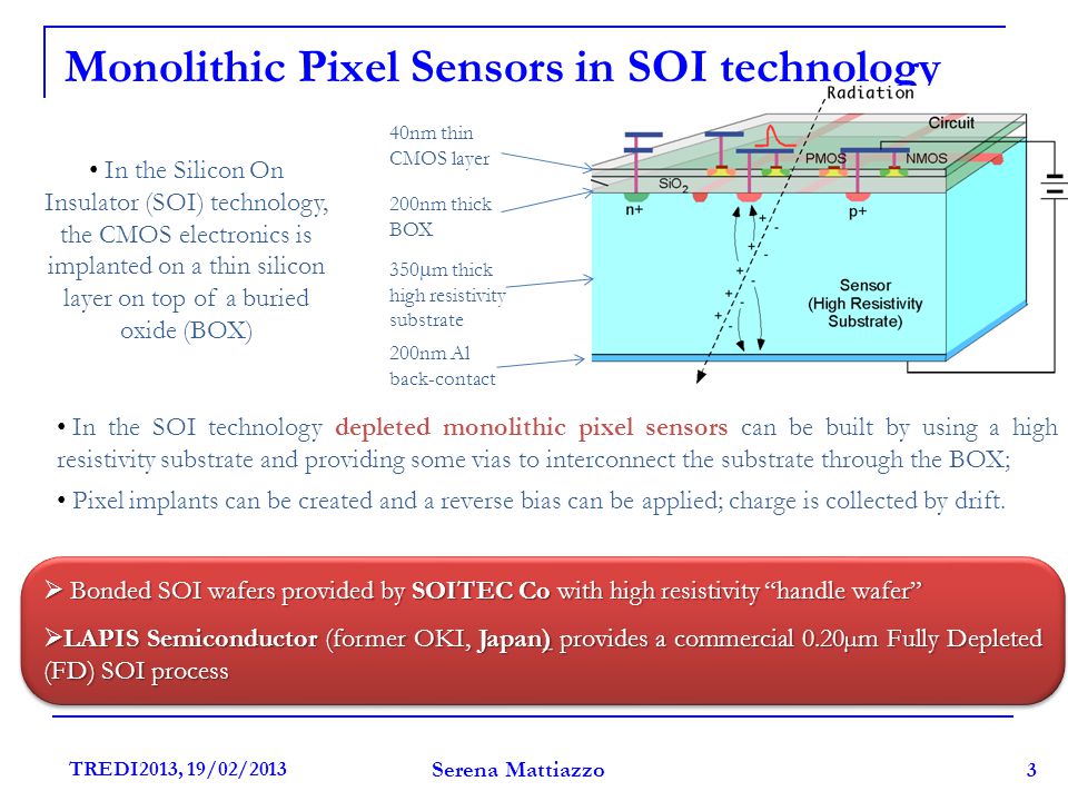
Development Of Monolithic Pixel Sensors In Silicon On Insulator Technology Serena Mattiazzo University Of Padova Italy D Bisello P Giubilato D Pantano Ppt Download
Research Topics
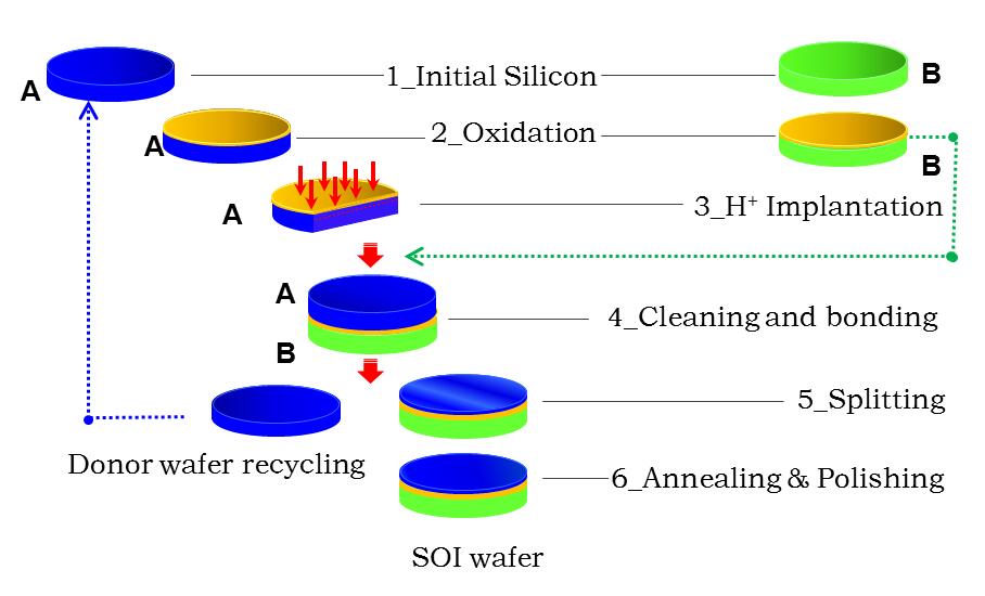
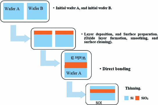
Pdf Fundamentals Of Wafer Bonding For Soi From Physical Mechanisms Towards Advanced Modeling

Figure 1 From 1 3 Mm Inas Gaas Quantum Dot Lasers On Silicon On Insulator Substrates By Metal Stripe Bonding Semantic Scholar


Process Flow For Cmos Compatible Fabrication Of Monocrystalline Silicon Download Scientific Diagram
Introduction To Silicon Photonics Springerlink

S O I Silicon On Insulator Presented By Arun Kumar Pandey Preetam Kumar Ppt Download

3d Memory Chips May Beat 3d Hybrid Memory Cube Memory Chip Semiconductor Mems
Https Encrypted Tbn0 Gstatic Com Images Q Tbn 3aand9gcrvnkgopd85kfb6hlkphmkvmydhz6oq6ccukpc2yhp6wbtot1vn Usqp Cau

Amazon Com Wafer Bonding Applications And Technology Springer Series In Materials Science Book 75 Ebook Alexe M G Sele U Alexe Marin Gosele Ulrich Kindle Store

Silicon On Insulator Technology Materials To Vlsi Springerprofessional De
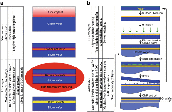
State Of The Art And Future Of Silicon On Insulator Technologies Materials And Devices Sciencedirect

Pressure Sensor Chip Fabricated In Soi Technology 1 A Pure Silicon Download Scientific Diagram

Silicon On Insulator Soi Technology For Micro Electromechanical Systems Mems And Nano Electromechanical Systems Nems Sensors Sciencedirect
Insulating Interlayer Boosts The Breakdown Voltage News

Technology Development For Soi Monolithic Pixel Detectors Sciencedirect

Silicon On Insulator Soi Technology Sciencedirect

Thick Film Silicon On Insulator Wafers Preparation And Properties Sciencedirect

Silicon On Insulator Technology Materials To Vlsi J P Colinge 9781402077739

Silicon On Insulator Technology Fabrication Of Soi Wafers Electronic Components
Https Static Aminer Org Pdf Pdf 000 233 781 Vertical Integration Of Submicron Mosfets In Two Separate Layers Of Pdf

Overview Of Semiconductor Technologies Key Semiconductor Technologies Bulk Silicon Soi Iii V And Ii Vi Semiconductors Economic Impacts Of Semiconductor Ppt Download
Wafer Bonding For Micro Electromechanical Systems Mems Springerlink

Ppt Overview Of Semiconductor Technologies Powerpoint Presentation Free Download Id 3491310
Fabrication Of Microdevices On Composite Pieozoelectric On Insulator Poi Wafers
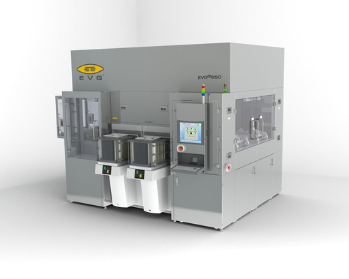
Ev Group Unveils Industry S First Wafer Bonding System For 450 Mm Silicon On Insulator Semiconductor Wafers

Plasma Activated Direct Bonding Of Diamond On Insulator Wafers To Thermal Oxide Grown Silicon Wafers Sciencedirect

The Smart Cut Technology Segment Is Estimated To Account For The Largest Share Of The Soi Market By Emma R Issuu
Http Journal Spqeo Org Ua Users Pdf N1 99 093 199 Pdf

Wafer Bonding

Epitaxial Quarter Iii V Wafer Bonded On Quasi Planarized Soi A Download Scientific Diagram

Technological Platform For Vertical Multi Wafer Integration Of Microscanners And Micro Optical Components Abstract Europe Pmc

Silicon On Insulator Soi Market Insulation Marketing Semiconductor
Https Encrypted Tbn0 Gstatic Com Images Q Tbn 3aand9gcsubbh9i500sgbpqiraqwywr Ia9ebqxcr9uk Zdbuyzjuh9nci Usqp Cau
Source : pinterest.com
